Development of a KABRA® Process Optimized for the Production of GaN Wafers
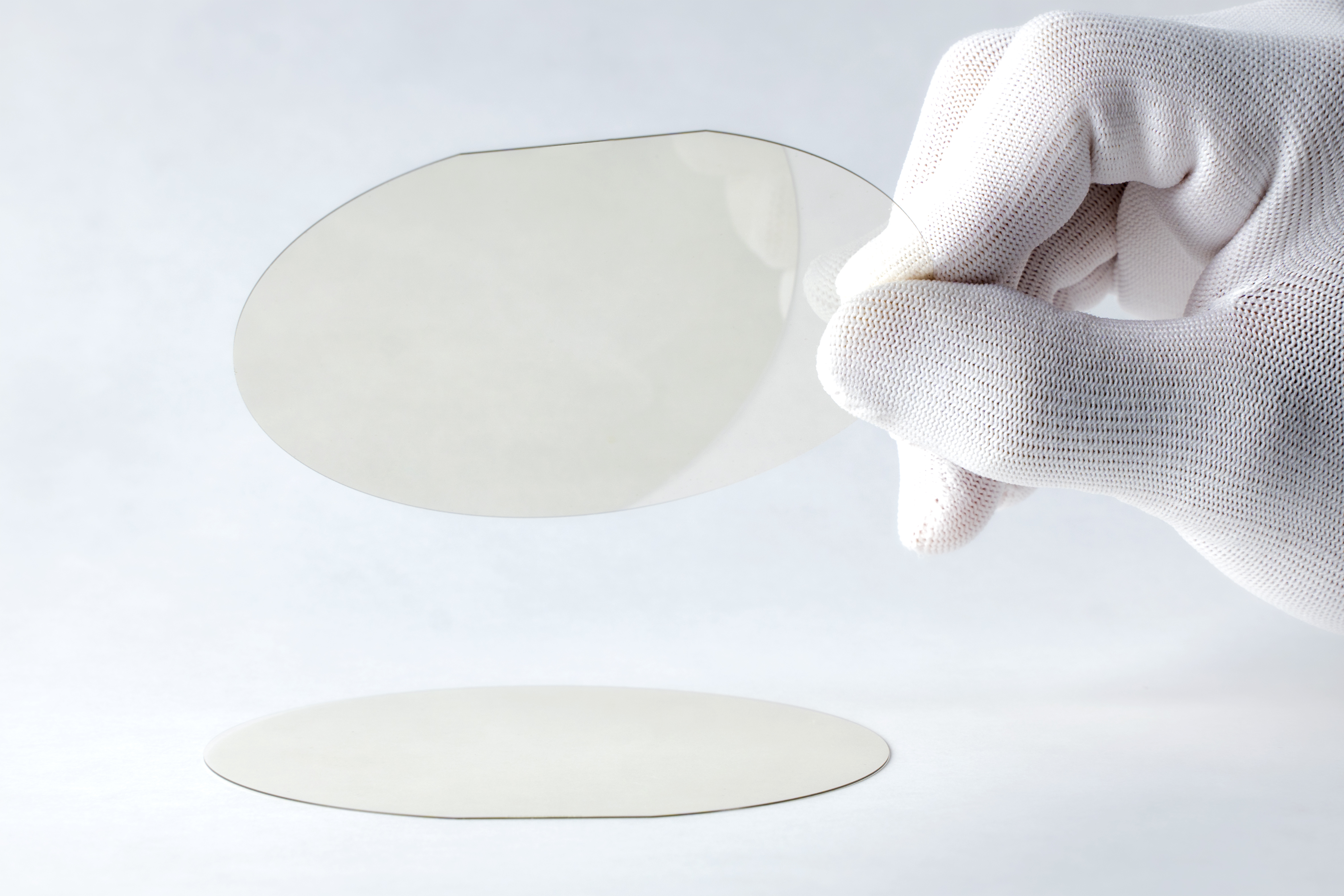
DISCO Corporation, a semiconductor manufacturing equipment manufacturer (Head Office: Ota-ku, Tokyo; President: Kazuma Sekiya), has used KABRA, an ingot slicing method using laser processing, and developed a process that is optimized for the production of GaN (gallium nitride) wafers. With this process, an increase in the number of GaN wafers produced and a decrease in production time can be achieved simultaneously.
Developmental Background
GaN, as a power device material, possesses features such as superior high-speed power conversion and low power loss during conduction, making it a promising contender for small-scale power sources and 5G base stations. It has also been in the spotlight as a material that responds to the worldwide demand for carbon neutrality. On the other hand, GaN requires time for crystal growth, and is a very delicate material as the ingots produced are small in diameter and thin.
Conventionally, the mainstream method to slice GaN ingots into wafers was to use a diamond wire saw. However, there were several problems when slicing with a wire saw, such as the processing time, material loss at the sliced sections that is thicker than the thickness of the wire used, and a low number of wafers produced due to material loss from the lapping process which is done after slicing to planarize the surface. These led to the wafers being expensive, and hindered the spread of GaN power devices.
From the time when the KABRA process was developed for the production of SiC (silicon carbide) wafers, DISCO has been receiving requests from many manufacturers to apply this process to GaN as well, which is a next-generation substrate material for power devices along with SiC. DISCO has been putting effort into R&D in order to realize a KABRA process optimized for GaN, and with this press release the company has announced it as a technology for mass-production.
High mass-productivity
Low material loss
- By controlling the laser focal point position in real time, slicing without thickness variation is possible
- Unlike the wire saw, the lapping process is unnecessary as there are no undulations after slicing
High throughput
- Developed a special optical system and processing method optimized for GaN
- Efficient creation of KABRA layer*1 due to short stage scanning distance
High yield
- Efficiently discharges the Nitrogen that is produced within the material and prevents wafer breakage by also creating a uniform KABRA layer near the edge of the ingot
*1: The processing mark and cleaved area created by focusing the laser within the material in the KABRA process
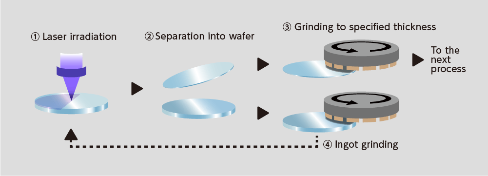
KABRA Process Flow for GaN Wafer Mass Production
- Laser is irradiated inside the ingot and KABRA layer is formed
- Ingot separated into wafer
- Wafer ground to specified thickness
- Ingot upper surface ground for next laser irradiation
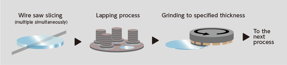
(Reference) Conventional Process Flow: Wire Saw
Superiority
Comparison of the Conventional Process and KABRA Process*2
1.Productivity Comparison
| KABRA Process*3 | Conventional Process*4 | |
|---|---|---|
| No. of wafers obtained from one ingot | 11 | 8 |
| No. of wafers produced in one hour | 6*5 | 1*6 |
| Material lost during slicing (per one wafer) |
None | Approx. 150 μm |
| Material lost during grinding (per one wafer, front and back surfaces) |
Approx. 60 µm (grinding processing marks) |
Approx. 100 μm |
2.Processing Time Comparison
| KABRA Process*3 | Conventional Process*4 | |
|---|---|---|
| Slicing process | Laser: 8 mins Separation: 8 mins |
25 hours (Simultaneous processing of multiple ingots) |
| Grinding wafer to specified thickness | Rough grinding: 10 mins Fine grinding: 10 mins |
6 hours (Simultaneous processing of multiple wafers) |
| Lapping process | Not necessary | Necessary |
*2: When producing wafers with a specified thickness of 400 µm (SEMI standard) from a 2 inch, 5 mm thick GaN ingot
*3: DISCO’s values are data obtained as of the timing of this press release
*4: When the lapping process is performed after slicing with a multi diamond wire saw. All values are general values obtained from users.
*5: No. of wafers produced assuming that four ingots are processed in parallel
*6: No. of wafer produced calculated from the time taken to perform wire saw slicing and the lapping process for four ingots simultaneously
Future Schedule
Test cuts and KKM services are available to be performed at the head office R&D center as and when requested.
Related Patents
34 (as of July 3, 2023, includes patents pending)
About DISCO Corporation
DISCO is a semiconductor equipment manufacturer that provides precision processing equipment, including dicing saws and grinders, and precision processing tools (blades and wheels) used for manufacturing semiconductors and electrical components. In addition to these products, as a result of pursuing optimal processing results for customers through the provision of the technology used in the equipment and tools, DISCO products and processing technologies have been widely adopted by device manufacturers and semiconductor subcontractors domestically and internationally. For details, please view the DISCO website www.disco.co.jp.
Contact
Please feel free to contact us with any questions or inquiries.