DFL7362: Stealth Dicing Laser Saw which Achieves Higher Throughput
DISCO CORPORATION (Head Office: Ota-ku, Tokyo; President: Kazuma Sekiya) has developed a stealth dicing (SD)*1 laser saw DFL7362 which supports Φ300 mm wafers. DFL7362 achieves the high-throughput processing of thin Si wafers by reducing the workpiece transfer time due to improvements to the platform and the processing axis speed. Furthermore, DFL7362 can be equipped with a wide range of optional functions which achieve both high processing-quality and high productivity, such as dual-use wafer and frame transferring, and kerf checks during processing. DFL7362 will be exhibited in SEMICON Japan 2017 held at Tokyo Big Sight from December 13 to 15.
*1 : Die singulation technology. An SD layer is formed on the dicing lines by focusing the laser beam inside the workpiece before singulation using die expansion or similar methods. Through the integration of the dicing technology that DISCO has developed and the SD engine that Hamamatsu Photonics Corporation has developed specifically for DISCO, stable, high-accuracy processing can be achieved.
Development Background
In recent years, with the widespread use of smartphones in Asia and growing needs for higher capacity and higher operation-speed storage and servers, the demand for flash memory is increasing. With flash memory, in order to stack die in the limited packaging space, it is necessary to cut out high-quality, thin die from the wafer. In order to meet these needs, DISCO provided the SDBG (Stealth Dicing Before Grinding) process*2 through DFL7361, which is already being used by many memory manufacturers throughout the world. The development of DFL7362 enables 30 % throughput improvement compared to the previous model and supports upgraded market needs.
*2 : Grinding the backside of the wafer and then performing singulation by thinning the wafer down until the designated thickness after performing the SD process.(Details)

Product Characteristics
- Stealth dicing equipment which supports Φ300 mm wafers
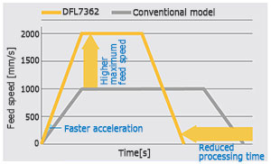
- Improves basic performance and achieves a high throughput (30 % increase to UPH)
- Improved acceleration rate and max. speed
- Reduced alignment time
- Reduced wafer replacement time
- A wide range of optional functions
- Dual-use wafer and frame transfer
- Reduced kerf check time
- Wafer thickness measurement function
- Equipment size: W 1,600 x D 2,760 x H 1,800 mm
Future Schedule
Sales will begin in December 2018
Contact
Please feel free to contact us with any questions or inquiries.