Wet Polishing (CMP etc.)
Solutions
With the reduction in height and size of IC packages, there is increased demand for thinner built-in die in silicon devices. Therefore, the stress relief process is carried out to improve die strength after wafer backgrinding. Furthermore, a polishing process is also required after backgrinding to improve performance for devices such as high luminance sapphire (Al2O3) substrate for LEDs, lithium tantalate (LiTaO3) / lithium niobate (LiNbO3) substrate for high-speed communication device SAW filters, and silicon carbide (SiC) substrate for power devices.
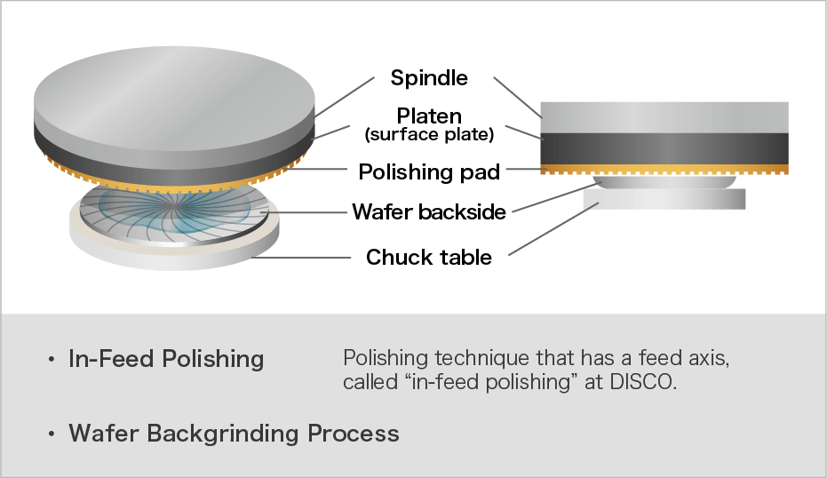
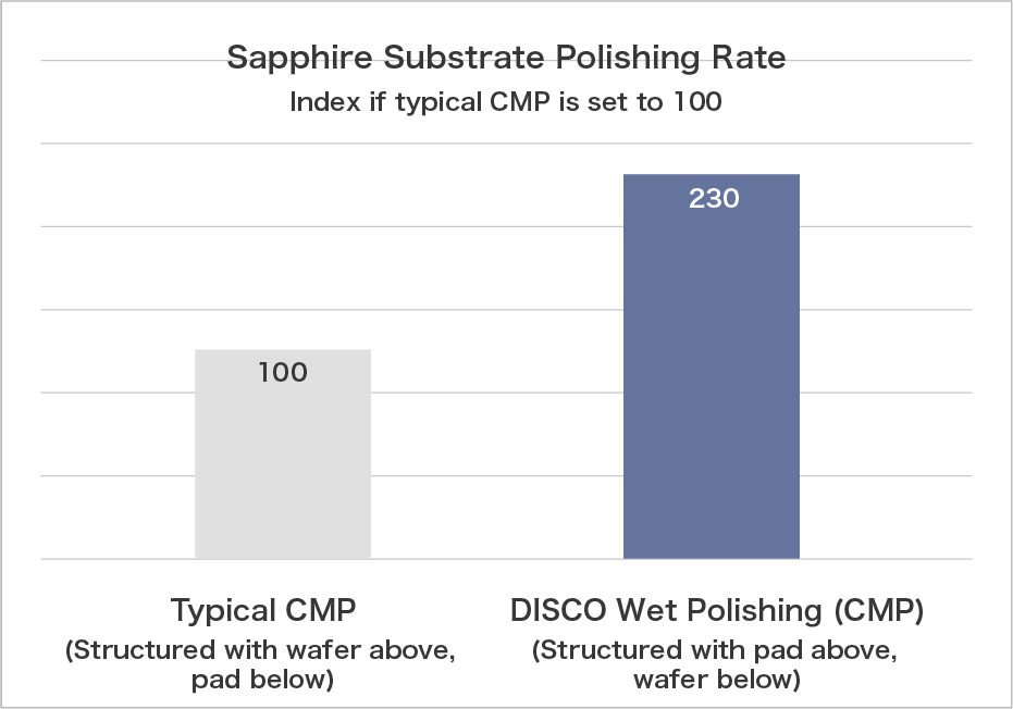
Typical CMP equipment places the wafer above and the polishing pad below. In contrast, DISCO equipment possess a feed axis and places the polishing pad above and the wafer below. This structure is called “in-feed polishing” and is used for both dry polishing and wet polishing (polishing technique using chemicals, among which the most well-known process is CMP). DISCO’s wet polishing, introduced here, realizes scratch reduction, mirror surface finish, and improvements to cleanliness. Furthermore, depending on the material, an Epi Ready* finish can be achieved.
*Epi Ready: surfaces and materials that enable epitaxial growth.

Characteristics of Wet Polishing Process
- Low-load, high-rotation polishing
Main Effects of Wet Polishing Process
- Mirror surface finish processing
- High cleanliness
- Depending on the material, low number of scratches and Epi Ready finish can be achieved
Application Examples
-
Polishing for wafer production (substrate manufacturing process)
- Silicon carbide (SiC)
- Sapphire (Al2O3)
- Lithium tantalite (LiTaO3) / Lithium niobate (LiNbO3)
-
Stress relief after backgrinding
- Silicon (Si)
- Sapphire (Al2O3)
- Lithium tantalate (LiTaO3) / Lithium tantalate (LiTaO3) on on silicon (Si)
- Gallium arsenide (GaAs)
- Indium phosphide (InP)
- Polishing before Cu-Cu bonding
- Regeneration processing of silicon (Si) wafers
Compatible Equipment
Our product line-up provides highly extensible capabilities that can be used to match our customer’s operating environment and can also be used for a wide range of applications.


Contact
Please feel free to contact us with any questions or inquiries.
-

Applications Support
A free-of-charge test cut is performed at an application lab to confirm whether achieving the customer's needs is possible.
Details -

Dicing and Grinding Service
It is effective in sample and prototype manufacturing during development or low-volume production. Designated engineers will provide support based on the desired leadtime and at reasonable cost.
Details