Dicing Thin Wafers
Solutions
In recent years, with the increased adoption of IC cards, RFID tags, and SIP (system in package) for cellular phones and other mobile products, the market for finished semiconductor die 50 µm thick or less has grown rapidly. This high demand has in turn made the processing of thin wafers an essential competence for many device manufacturers. To provide the processing results that these companies require, DISCO continuously researches and develops the machines, blades, and applications that make thin wafer dicing a reality.
Blades
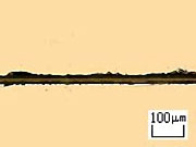
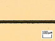
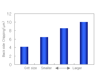
As a workpiece grows thinner, backside chipping caused during the dicing process also tends to increase. Photos 1 and 2 show backside chipping in a 25 µm-thick silicon wafer, the backside of which was dry polished prior to dicing. For the workpiece in Photo 1, a #2000 blade was employed, typical for standard-thickness dicing; backside chipping, however, is substantial. For the workpiece in Photo 2, a #4800 blade (much finer grit) was employed; backside chipping has been greatly reduced. In general, as Graph 1 indicates, a finer-grit blade imparts less of a shock to the workpiece, thereby reducing backside chipping.
-
Photo 1: Typical Grit Size (#2000)
-
Photo 2: Small Grit Size (#4800)
Processing Conditions
As stated above, it is generally advisable to dice thin wafers with an extremely fine-grit blade. But
because these blades have reduced cutting power, they can be affected by films, TEGs, and other elements
of the wafer frontside. Clogging can result, in turn compromising processing quality on the wafer
backside. In such a case, the use of a step cut (instead of single-pass dicing) often solves the
problem. Further, when performing blade dicing with a view to stable, long-term processing, it is
essential to maintain a consistent processing load and preserve the self-sharpening mechanism of the
blade.
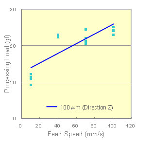
In the case of thin wafer dicing, the volume of material being ground by the blade does not contribute
significantly to the processing load; therefore, this load must be raised by adjusting the processing
conditions themselves. Graph 2 displays the relationship between feed speed and processing load. Grit
size, feed speed, and spindle speed are closely interrelated processing factors that require knowledge
and experience to adjust. DISCO performs careful and detailed experiments that allow a perfect match
between dicing processing conditions and customers’ thin semiconductor workpieces.
DISCO Short Kerf Check Function (Patent Pending)
In the typical kerf check function, spindles Z1 and Z2 cut in separate areas with kerfs checked
individually (it is difficult to check both kerfs simultaneously, as the Z2 kerf becomes hard to measure).
In the case of a step cut, however, the Z2 blade, which does not normally cut the surface of the wafer,
can encounter films, TEGs, etc., and incur damage. This damaged Z2 blade may then cause backside chipping
and other problems.
DISCO's Short Kerf Check function can help solve this problem. In this function, the Z2 blade cuts with a
shortened stroke; the kerf is then measured and the information processed. Because of the shortened
stroke, the Z2 blade incurs minimal damage and does not become a cause of increased backside chipping.
Through the proper blade, processing conditions, and the DISCO Short Kerf Check function, it is possible
to dice thin wafers with extremely high processing quality. Please contact your DISCO representative for
further details about thin wafer dicing and DISCO's premier applications support.
Contact
Please feel free to contact us with any questions or inquiries.
-

Applications Support
A free-of-charge test cut is performed at an application lab to confirm whether achieving the customer's needs is possible.
Details -

Dicing and Grinding Service
It is effective in sample and prototype manufacturing during development or low-volume production. Designated engineers will provide support based on the desired leadtime and at reasonable cost.
Details